Voiding
Voiding is a hot topic for many electronics manufacturers. Voids in solder joints can create mechanical weaknesses which leads to cracks in the solder joint.
Voids can also interfere with heat transfer away from a component which leads to thermal failure. Many electronics manufacturers are looking for ways to minimize voiding in their solder joints. FCT Solder is happy to provide solutions to mitigate voiding.
Voiding is caused by a variety of factors. In some cases, multiple factors work together to create voids. The most common factors that cause voiding will be discussed here.
First and foremost, solder paste contributes to voiding. Gasses generated from the solder paste are trapped in the solder joint creating voids. Some solder pastes are prone to generate higher voiding than others.
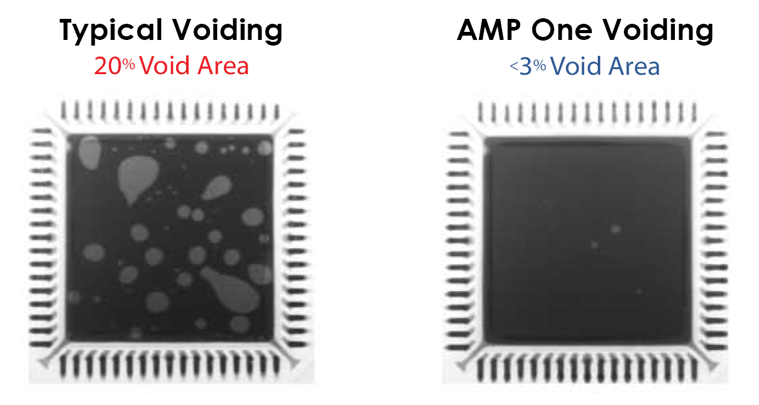
Newer solder pastes have been formulated with the specific goal of minimizing voiding. Our no clean, lead-free solder paste called Amp OnePT is a good example of an ultra-low voiding solder paste (Figure 1).
The reflow profile must be tuned to work with the solder paste in order to minimize voiding. Most solder paste manufacturers formulate solder pastes to work with standard ramp-to-spike (RTS) and ramp-soak-spike (RSS) profiles.
Each solder paste is different and reacts differently to the reflow profile in terms of voiding (Figure 2).
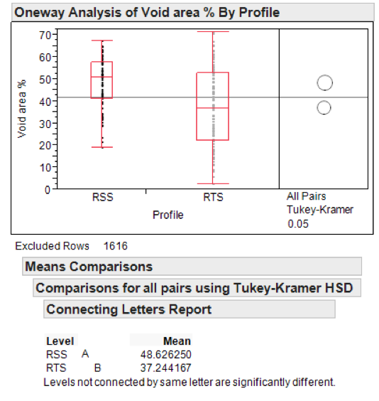
Void area is significantly higher for the RSS profile than for the RTS profile with this solder paste. We would recommend using an RTS profile with this particular solder paste in order to minimize voiding.
Again, the reflow profile must be tuned for the solder paste that you are using.
Wetting of the solder on the component leads / pads and circuit board pads play a role in voiding. Poor wetting creates gaps in the solder joint, which by definition are voids.
Some solder pastes wet and flows better than others which tends to minimize voiding.
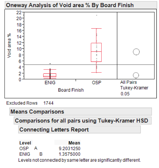
Organic Solderability Preservative (OSP) type surface finishes are typically more difficult to wet than Electroless Nickel Immersion Gold (ENIG) surface finishes. There is a clear difference in voiding between these surface finishes with some solder pastes (Figure 3).
This particular solder paste wets and spreads much better on ENIG than OSP, which leads to lower voiding with the ENIG surface finish.
Stencil design can have a large impact on voiding especially when the circuit board design lends itself to voiding. Most electronics assemblers do not have the ability to change the circuit board design but the stencil can be changed to compensate for the circuit board.
Via in pad design is common for bottom terminated component thermal pads. Via holes are typically not plugged and therefore contain air or residues from previous processes.
During reflow, gasses from the via holes escape up into the solder joint causing voiding. It has been shown that printing solder paste around the vias and including gas escape routes in the solder paste print can reduce voiding.
FCT Solder manufactures solder pastes and stencils to solve problems like voiding in solder joints.
To learn more about solder paste and its evaluation process, read on here.
Still interested in learning about voiding solutions? Click the button below.
Solder Voiding Prevention
Issue Description: Commonly caused by gas pockets trapped inside the solder joint.
1) Modify the reflow profile to generate less volatile material and to give more time for the gas to escape.
Increasing soak time will reduce voiding for some solder pastes.
Increasing soak time will drive off more of the low boiling volatiles from the solder paste prior to reflow.
Increasing peak temperature will reduce voiding for some solder pastes. Increasing peak temperature gives more heat and time above liquidus which allows volatile materials to escape before the solder joint solidifies.
Reflow Profile for Voiding
The reflow profile can contribute to voiding in solder joints. If the ramp rate is too high then volatile materials may not be completely driven off and can lead to voiding. High ramp rates or short reflow profiles can lead to incomplete wetting or spread of the solder paste.
High peak temperatures or long reflow profiles can cause less than optimal wetting, and the flux may generate additional gases which can lead to voiding. The reflow profile must be tuned to work with the solder paste in order to minimize voiding.
2) Modify the stencil to give gas escape routes under components (QFN thermal pads are common trouble spots).
5-dice, window pane, cross hatch, and radial solder paste deposits all provide gas escape routes.
Clearances can be created around via holes so that solder paste is not pulled into the via hole during reflow.
Stencil Design to Reduce Voiding
Modification of the stencil design is one possible solution to voiding. Our partner, BlueRing Stencils can offer specific stencil designs to minimize voiding. Bottom terminated components require the solder paste deposit to be broken up with a crosshatch pattern.
This gives channels for gasses to escape from the solder joint before the solder freezes. When using via-in-pad designs, solder paste can be printed around the via holes rather than directly over them. This prevents solder paste from flowing down into the via holes and minimizes voiding.
3) Switch to a solder paste formulation that has a lower tendency to form voids.
Solder paste formulations with lower volatile content obviously will create lower voiding. For example, WS888 solder paste has lower volatile content than WS889 and will have a reduced tendency to form voids.
No clean solder pastes typically will give lower voiding than water-soluble solder pastes. No clean solder pastes usually have lower volatile content than water solubles. No clean solder pastes also have a much lower tendency to absorb moisture from the air. Moisture absorption into the solder paste results in higher voiding.
Solder alloys with a melting range generate lower voiding than eutectic solder alloys. The melting range gives a longer time for complete coalescence of the solder powder, which allows gas to escape before the joint becomes fully liquid. This is easily accomplished in lead-free solder pastes by using an alloy with some silver like SAC305.
Using Solder Paste to Reduce Voiding
One major contributor to voiding in solder joints is solder paste. Solder pastes contain ingredients that volatilize during reflow. These volatile materials become gas bubbles that can be trapped in the solder joint. Different solder pastes also wet and spread differently.
Incomplete wetting or spreading on the board pad and component surfaces leads to voiding. FCT Assembly has formulated solder pastes with the specific intention of reducing voiding potential. Our ultra low voiding solder pastes have reduced volatile content and optimized wetting.
Voiding Solutions
FILL THE VOID
Voids in solder joints are a concern for many electronics manufacturers. They create weakness in the solder joints which can lead to mechanical failure. Voids can slow or limit heat transfer away from the component which can lead to thermal failure. Voids can also interfere with electrical signal flow creating problems with the function of the circuit board. Minimization of voiding is beneficial for the life and function of the circuit assembly.

Fill the Void II: An Investigation into Methods of Reducing Voiding
Voids in solder joints plague many electronics manufacturers. Do you have voids in your life? We have good news for you, there are many excellent ways to “Fill the Void.” This paper is a continuation of previous work on voiding in which the following variables were studied: water-soluble lead-free solder pastes, a variety of stencil designs, and reflow profiles. Quad Flat No-Lead (QFN) component thermal pads were used as the test vehicle. The voiding results were summarized and recommendations were made for reduction of voiding.

Fill the Void III
This study is part three in a series of papers on voiding in solder joints and methods for mitigation of voids. In this study several new variables were tested and compared to previous data on voiding. A new circuit board design was used which is different than the circuit board used in previous studies. The new circuit board design includes two sizes of QFNs (Quad Flat No Lead), BGA’s (Ball Grid Array), and LGA (Land Grid Array) components which are susceptible to voiding.

Fill the Void IV
Voids are a plague to our electronics and must be eliminated! Over the last few years we have studied voiding in solder joints and published three technical papers on methods to “Fill the Void.” This paper is part four of this series. The focus of this work is to mitigate voids for via in pad circuit board designs.

Fill the Void V
Voiding in solder joints has been studied extensively, and the effects of many variables compared and contrasted with respect to voiding performance. Solder paste flux, solder powder size, stencil design, circuit board design, via-in-pad design, surface finish, component size, reflow profile, vacuum reflow, nitrogen reflow and other parameters have been varied and voiding quantified for each. The results show some differences in voiding performance with respect to most of these variables but these variables are not independent of each other. Voiding in solder joints is a complex issue that often requires multiple approaches to reduce voiding below required limits. This paper focuses on solutions to voiding for commonly used bottom terminated components (BTCs).
