As electronics (and printed circuit boards) get smaller with every passing year, SMT manufacturers face some big new challenges. One thing’s for sure: the trend towards smaller, more compact electronics isn’t going away.
Smart manufacturers are addressing these issues now to keep pace with these changes and prepare for the future. One major obstacle everyone in our industry must address is solder bridging.
What is solder bridging, and why is it a problem?
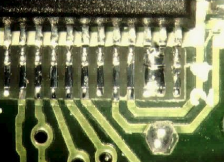
Solder bridging is a common SMT defect. It occurs when solder flows between connectors and causes a “bridge,” or short. It’s not always immediately obvious when solder bridging happens… but it can wreak havoc on the component or device.
Bridging can occur at multiple parts of the manufacturing process. Sometimes, it occurs at the solder paste print, when solder paste is squeezed between the PCB and stencil and deposits extra paste.
It can also be caused by PCB fabrication problems, the placement pressure of a component, settings of the reflow oven, and more.
Whether bridging is caused by issues with the board design, too much paste, or another problem, it’s definitely a headache for manufacturers.

How to reduce solder bridging
Because solder bridging is caused by a myriad of issues, there’s no one sure-fire way to eliminate it. But it definitely CAN be stopped! We’ve studied ways to reduce bridging, and we’re happy to share some of our top strategies with you.
1) Change the circuit board design.
This isn’t always possible; contract manufacturers don’t always have a say in optimizing board design. But when it is possible, it’s one of the most effective ways to reduce bridging, especially by adjusting aperture width and area ratio.
Additionally, solder mask dams can be added between fine pitch pads to prevent solder from bridging. Solder mask defined pads can also prevent bridging, especially in tight pitch areas like BGAs and LGAs.
2) Modify the reflow profile.
Increasing the time above liquidus will allow more time for the solder to flow where it is supposed to be. Once the pads and leads reach the same temperature, the solder will wet both, causing the solder to move to the intended location.
Liquid solder tends to flow to the warmer surface first. The component leads can be warmer than the pad due to their lower thermal mass and increased air flow around the lead. Increasing soak time will equalize temperatures across the assembly and reduce the tendency for solder to flow to the warmer surfaces.
3) Reduce the likelihood of off-contact solder paste printing.
Try modifiying the stencil design to reduce the amount of solder paste in trouble areas. You can also change the board design to eliminate the causes of off contact printing. Legend marking ink next to solder mask defined pads can cause off contact of several mils resulting in much higher solder paste volume.
4) Reduce the solder paste volume or component lead size.

A stencil modification to reduce the volume or location of the solder paste on the pad can dramatically reduce bridging. After all, solder bridging is an issue that occurs when solder gets somewhere it shouldn’t be.
Using a component with increased leads will also reduce the potential for the solder to flow up and between leads. Increasing the component lead size will help to take up more solder volume preventing it from spilling over between the pads. One common cause of solder bridging is when a pad is designed for a long footed lead but an alternative component is used with a shorter lead. The solder must wet relatively more area on the pad, leaving less volume to flow up the lead.
Thermal differences are especially challenging with gull wing leads. During reflow, solder paste can pool and cause bridges. Try modifying the stencil to reduce the paste volume printed on the land pad.
Engineering Support
Experiencing bridging issues? Need help solving a solder problem?
Give our engineers a call to talk things through and find a solution.
More resources to help avoid solder bridging SMT defects
Need more help? These technical papers from our field application engineers offer more insight and guidance into addressing problems that diminish SMT assembly yields, including bridging.
Improve SMT Assembly Yields Using Root Cause Analysis in Stencil Design
By reducing first pass defects, manufacturers save money and time, as well as improving their products’ reliability. Yield boils down to those three areas (cost, delivery, and reliability), and it’s a key element for efficient, profitable assembly.
Solder paste printing is a major culprit for yield problems that SMT manufacturers face… and it’s only exacerbated by the trend towards smaller and smaller form factors.
This paper takes a hard look at the defects that affect SMT yields in the printing process and breaks down their root causes. Additionally, it takes a look at how outer layer copper weight and surface treatment affect printability, as well as experiments in leadless and emerging components. You’ll also find root cause analysis for several common SMT defects.
SMT Assembly Challenges and Proven Solutions for Improving Yields
As advanced PCB manufacturing and component designs become more and more common, SMT assemblies are also growing more complicated. There’s a definite trend towards “hybrid” assemblies that use both old and new technologies. This paper takes a look at those challenges to discover how manufacturers can maintain and increase their yields.


